
via-in-pad issue (standard technology)
Views : 2675
Author : meidear
Update time : 2020-03-10 16:51:49
DFM/DFA/DFT Tips&Tricks - TIP #03 => via-in-pad issue (standard technology)
Whenever possible, always use enough clearance for the solder mask between the via and the copper pad to prevent solder flow into the via hole and can cause the solderability issues during the assembly and manufacturing process.
This note applies only to standard technology, especially typical 2-layer PCBs.
Please remember, that for multilayer HDI PCBs there is a similar via-in-pad technique (mostly used for small pitch BGAs), but that vias are additionally filled and plated.
There are some exceptions, such as RF circuits, high-current designs or BGA layouts, where that recommendation can be omitted.
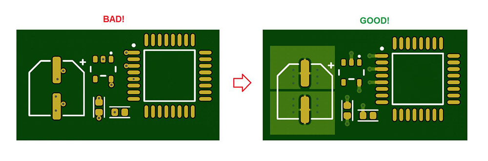

Related News

The Prevalence of Mid-High TG Materials in Multilayer PCB Fabrication
Jul .17.2025
In the manufacturing of multilayer printed circuit boards (PCBs), mid-high glass transition temperature (TG) materials have become the norm. This article aims to explore the reasons behind this industry preference.

NEWS FLASH: Guangzhou International Lighting Exhibition 2025 Signals Major Shifts for PCB Industry in Lighting & Beyond
Jun .12.2025
Guangzhou, China – June 12, 2025
(Reporting Live from Guangya Expo 2025)
(Reporting Live from Guangya Expo 2025)

Comparison of LDI and CCD Exposure Systems
Apr .03.2025
In the PCB (Printed Circuit Board) manufacturing process, exposure is a critical step. Many PCB manufacturers like meidearpcb utilize CCD semi-automatic exposure machines for this process.

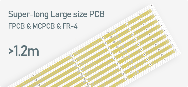
LED lighting PCB (Printed Circuit Board) Solutions
Jan .01.2025
LED lighting PCB (Printed Circuit Board) solutions
CEM-3 Thermal conductive material
IMS pcb Flexible pcb Copper-base pcbs
CEM-3 Thermal conductive material
IMS pcb Flexible pcb Copper-base pcbs

